SC-OBC Module A1 Product Manual
1. Introduction
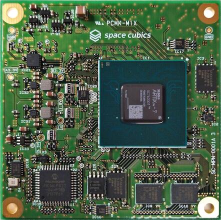
The SC-OBC Module A1 is an On-Board Computer (OBC) designed for use in CubeSats that are 3U in size or larger.
The SC-OBC Module A1 is a system that uses a Xilinx Artix-7 FPGA as its primary processing unit, featuring an embedded ARM Cortex-M3 core implemented within the FPGA. By using an FPGA, the type and number of interfaces can be flexibly customized for each CubeSat. In addition, implementing user-defined IP enables specialized processing without utilizing CPU resources, which can enhance overall system performance.
The SC-OBC Module A1 includes a PIC16LF877 sub-microcontroller as a secondary system management unit, operating independently from the main processor. This sub-microcomputer, known as the Timing, Reset, Config & Health Controller (TRCH), manages the system prior to FPGA startup and monitors for anomalies after the FPGA has started. The SC-OBC Module A1 features an automatic recovery mechanism that utilizes TRCH to restore the system in the event of an abnormality.
2. Product Overview
2.1. Specifications
| Features | Description |
|---|---|
Main Device |
Xilinx Artix-7 (XC7A200T-1FBG676I) |
- Logic Cells: 215,360 |
|
- CLB slice count (4 LUT, 8 F/F): 33,650 |
|
- Maximum Distributed RAM in CLBs: 2,888 Kb |
|
- DSP48E1 slices: 740 |
|
- Block RAM: 36 Kb x 365 (18 Kb x 730) |
|
- CMTs: 10 |
|
- XADC: 1 (for FPGA die temperature measurement) |
|
- I/O Banks: 10 |
|
Main CPU |
ARM Cortex-M3 Design Start FPGA Xilinx Edition r0p1 |
- CPU Revision r2p1 |
|
- ARMv7-M architecture profile |
|
- Maximum operation frequency up to 48 MHz (T.B.D.) |
|
TRCH |
PIC16LF877 8 bit RISC CPU |
- operation frequency: 4 MHz |
|
FPGA Source Clock |
24 MHz |
On Chip SRAM |
32 kByte of FPGA BlockRAM |
On Borad SRAM |
4 MByte Asynchronous Static RAM (CY7C1061GE) |
- ECC Memory Protection |
|
- Memory Scrubbing |
|
Configuration Flash Memory |
32 MByte/Redundancy (NOR Flash: S25FL256L) |
Data Store Flash Memory |
32 MByte/Redundancy (NOR Flash: S25FL256L) |
FeRAM |
512 kByte x 2 (CY15B104QSN) |
Control Area Network (CAN) |
Conforms to the ISO 11898-1, CAN2.0A, and CAN2.0B standards. Supports bit rates up to 1 Mb/s. |
Space Communication Bus (SCBus) |
Compliant with the USB-based communication interface proposed by Space Cubics (T.B.D.) |
- Supports bit rates up to 12 Mbps (USB Full-Speed) |
|
I2C Interface |
Accessible from FPGA and TRCH x 1 |
Serial Interface |
TRCH UART Interface x 1 |
(Connection to the FPGA can be configured based on the selected hardware options.) |
|
FPGA User IO |
User IO Group 1 x 16 pin (variable IO voltage) |
User IO Group 2 x 16 pin (variable IO voltage) |
|
User IO Group 4 x 6 pin, Cortex-M3 JTAG compatible (3.3V fixed) |
|
TRCH User IO |
User IO Group 3 x 3 pin (3.3V fixed) |
(Connection to the FPGA can be configured based on the selected hardware options.) |
|
Power Supply Voltage |
DC 5.0V ± 10% |
Power Consumption |
2.0 W (Max) |
Operating temperature range |
-40℃ to +80℃ |
External Dimensions |
70 mm x 70 mm |
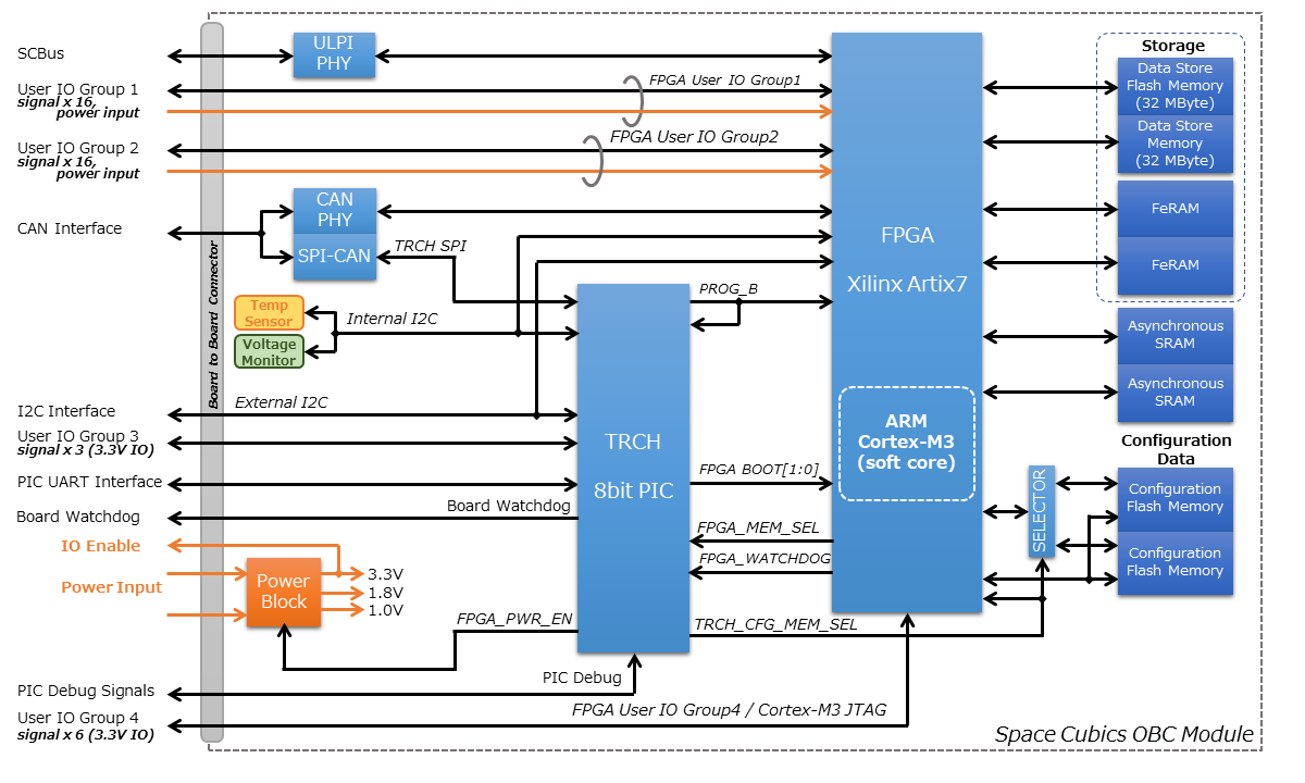
2.2. Block Diagram
The SC-OBC Module A1 is composed of two boards—an OBC module and an IO board—providing high flexibility by leveraging the capabilities of the FPGA.
The OBC Module provides versatile functionality that remains consistent regardless of interface changes in systems using the SC-OBC Module A1. The IO Board, on the other hand, handles functions that directly impact system configuration—such as transceiver ICs and protocol converter ICs—ensuring compliance with the electrical requirements of the interface.
Users of the SC-OBC Module A1 can accommodate new satellites by redesigning the IO Board, allowing flexibility even when the satellite system changes. Although satellite systems may differ, systems sharing the same OBC Module can still reuse much of their software assets.
The OBC Module and IO Board are connected via an 80-pin board-to-board connector.
3. Electrical Specifications
3.1. Absolute Maximum Ratings
| Item | Symbol | Minimum | Maximum | Unit | Conditions / Notes |
|---|---|---|---|---|---|
Power supply voltage |
VIN_A, VIN_B |
-0.3 |
10.0 |
V |
|
FPGA I/O bank power supply voltage |
VDD_UIO1, VDD_UIO2 |
-0.5 |
3.6 |
V |
|
Input/output voltage (excluding ULPI, CAN, and ICSP_MCLR_B signals) |
VI, VO |
-0.3 |
OVDD + 0.3 |
V |
OVDD = VDD_3V3_SYS, VDD_3V3_IO, VDD_UIO1, and VDD_UIO2 |
Input voltage (ULPI_DP and ULPI_DM signals) |
VI_ULPI |
-0.3 |
5.25 |
V |
|
Input voltage (CANH and CANL signals) |
VI_CAN |
-7 |
16 |
V |
|
Input voltage (ICSP_MCLR_B signals) |
VI_ICSP_MCLR_B |
0 |
14 |
V |
|
FPGA junction temperature |
Tj_FPGA |
125 |
℃ |
||
Operating temperature |
Topr |
-40 |
85 |
℃ |
no condensation |
Storage temperature |
Tstg |
-40 |
85 |
℃ |
Absolute maximum rating defines the value that must not be exceeded, even momentarily, during any operating or testing condition. Exceeding absolute maximum ratings can cause permanent damage to the device. Please operate with a sufficient safety margin below the specified values.
3.2. Recommended Operating Conditions
| Item | Symbol | Minimum | Standard | Maximum | Unit | Conditions / Notes |
|---|---|---|---|---|---|---|
Power supply voltage |
VIN_A, VIN_B |
4.5 |
5.0 |
5.5 |
V |
|
FPGA I/O bank supply voltage |
VDD_UIO1, VDD_UIO2 |
1.14 |
3.465 |
V |
Power should be switched on and off simultaneously with VDD_3V3_IO, or only when VDD_3V3_IO is supplying 3.3V. |
|
Operating temperature |
Topr |
-40 |
25 |
80 |
℃ |
no condensation |
3.3. Electrical Properties
| Item | Symbol | Minimum | Standard | Maximum | Unit | Conditions / Notes |
|---|---|---|---|---|---|---|
Over-voltage protection (OVP) threshold voltage |
Vovp_th |
6.0 |
V |
|||
Under-voltage lockout (UVLO) threshold voltage |
Vuvlo_th_h |
4.1 |
V |
When VIN_A and/or VIN_B rise |
||
Vuvlo_th_l |
3.6 |
V |
when VIN_A and/or VIN_B drop |
|||
Over-current detection |
Iocp_th_VIN_A |
1.3 |
1.6 |
1.9 |
A |
VIN_A |
Iocp_th_VIN_B |
1.3 |
1.6 |
1.9 |
A |
VIN_B |
|
Iocp_th_VDD_3V3_SYS |
N/A |
N/A |
N/A |
A |
VDD_3V3_SYS |
|
Iocp_th_VDD_3V3_IO |
0.42 |
0.57 |
0.73 |
A |
VDD_3V3_IO |
|
I/O power supply voltage |
VDD_3V3_SYS |
2.97 |
3.3 |
3.465 |
V |
Iout_max = 100mA |
VDD_3V3_IO |
2.97 |
3.3 |
3.465 |
V |
Iout_max = 300mA |
3.4. Power Circuit Configuration
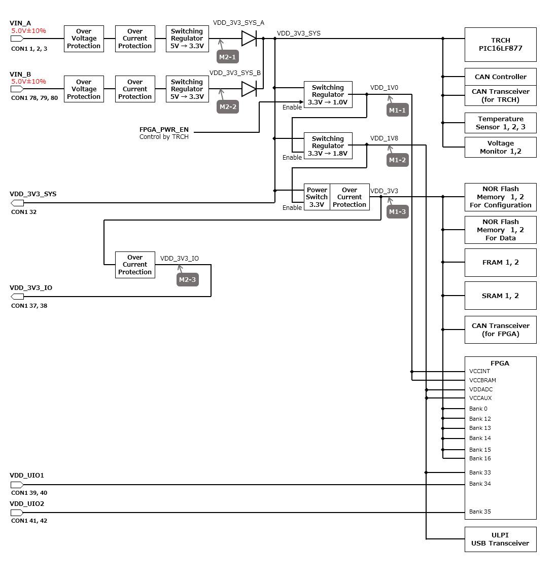
The power supply circuit configuration of the OBC module is shown below. Power supply inputs VIN_A (CON1 pins 1, 2, 3) and VIN_B (CON1 pins 78, 79, 80) operate redundantly, generating VDD_3V3_SYS_A and VDD_3V3_SYS_B independently. These two power lines are combined into VDD_3V3_SYS through ideal diodes and supply power to the TRCH and other components. Additionally, VDD_3V3_SYS is also provided externally via the IO board interface (CON1 pin 32). Since VDD_3V3_SYS is shared with internal circuits, its maximum current usage should not exceed 100 mA.
FPGA_PWR_EN activates each power IC, supplying power to internal circuits and external output pins as needed.
The generated power output nodes are equipped with current and voltage monitors, enabling power status monitoring from both TRCH and FPGA (M1-1, M1-2, M1-3, M2-1, M2-2, M2-3).
VDD_3V3_IO is supplied externally through the IO board interface (CON1 pins 37 and 38) and includes overcurrent protection rated at 300 mA.
4. Interface Specifications
This section outlines the interface specifications for the SC-OBC Module A1 Module.
4.1. CON1 (IO Board Interface)
The IO Board interface connects the OBC Module and the IO Board. This interface uses a Panasonic 0.5 mm pitch 80-pin connector (model number: AXK6S80547YG). Use a socket with a mating height of 5 mm, 5.5 mm, or 8 mm to connect with the corresponding IO board.
Refer to the Board Layout Diagram for connector locations.
| Pin Number | Pin Name | I/O | Power Domain | Description |
|---|---|---|---|---|
1 |
VIN_A |
Power |
- |
power supply (VIN_A) |
2 |
VIN_A |
Power |
- |
power supply (VIN_A) |
3 |
VIN_A |
Power |
- |
power supply (VIN_A) |
4 |
ULPI_DP |
Inout |
- |
SC Bus D + signal |
5 |
ULPI_DM |
Inout |
- |
SC Bus D - signal |
6 |
GND |
Power |
- |
power supply (GND) |
7 |
UIO1_00 |
Inout |
VDD_UIO1 |
User IO1 Bit 0 signal is connected to FPGA pin IO_L13P_T2_MRCC_34 (pin: R3). |
8 |
UIO1_01 |
Inout |
VDD_UIO1 |
User IO1 Bit 1 signal is connected to FPGA pin IO_L13N_T2_MRCC_34 (pin: P3). |
9 |
UIO1_02 |
Inout |
VDD_UIO1 |
User IO1 Bit 2 signal is connected to FPGA pin IO_L14P_T2_SRCC_34 (pin: P4). |
10 |
UIO1_03 |
Inout |
VDD_UIO1 |
User IO1 Bit 3 signal is connected to FPGA pin IO_L14N_T2_SRCC_34 (pin: N4). |
11 |
UIO1_04 |
Inout |
VDD_UIO1 |
User IO1 Bit 4 signal is connected to FPGA pin IO_L11P_T1_SRCC_34 (pin: M2). |
12 |
UIO1_05 |
Inout |
VDD_UIO1 |
User IO1 Bit 5 signal is connected to FPGA pin IO_L11N_T1_SRCC_34 (pin: L2). |
13 |
UIO1_06 |
Inout |
VDD_UIO1 |
User IO1 Bit 6 signal is connected to FPGA pin IO_L10P_T1_34 (pin: H2). |
14 |
UIO1_07 |
Inout |
VDD_UIO1 |
User IO1 Bit 7 signal is connected to FPGA pin IO_L10N_T1_34 (pin: H1). |
15 |
GND |
Power |
- |
電源(GND) |
16 |
UIO1_08 |
Inout |
VDD_UIO1 |
User IO1 Bit 8 signal is connected to FPGA pin IO_L7P_T1_34 (pin: K1). |
17 |
UIO1_09 |
Inout |
VDD_UIO1 |
User IO1 Bit 9 signal is connected to FPGA pin IO_L7N_T1_34 (pin: J1). |
18 |
UIO1_10 |
Inout |
VDD_UIO1 |
User IO1 Bit 10 signal is connected to FPGA pin IO_L9P_T1_DQS_34 (pin: N1). |
19 |
UIO1_11 |
Inout |
VDD_UIO1 |
User IO1 Bit 11 signal is connected to FPGA pin IO_L9N_T1_DQS_34 (pin: M1). |
20 |
UIO1_12 |
Inout |
VDD_UIO1 |
User IO1 Bit 12 signal is connected to FPGA pin IO_L18P_T2_34 (pin: U2). |
21 |
UIO1_13 |
Inout |
VDD_UIO1 |
User IO1 Bit 13 signal is connected to FPGA pin IO_L18N_T2_34 (pin: U1). |
22 |
UIO1_14 |
Inout |
VDD_UIO1 |
User IO1 Bit 14 signal is connected to FPGA pin IO_L1P_T0_34 (pin: K3). |
23 |
UIO1_15 |
Inout |
VDD_UIO1 |
User IO1 Bit 15 signal is connected to FPGA pin IO_L1N_T0_34 (pin: J3). |
24 |
GND |
Power |
- |
power supply (GND) |
25 |
UIO3_00 |
Inout |
VDD_3V3_SYS / VDD_3V3_IO[1] |
Power domains differ depending on hardware options. See “Hardware options and IO connections” [fuzzy:*Hardware options and IO connections]. User IO3 Bit 0 signal is connected to RD4/PSP4 of the PIC16LF877. This can be reassigned to FPGA pin IO_L23P_T3_12 (pin: Y15) via hardware configuration options. |
26 |
UIO3_01 |
Inout |
VDD_3V3_SYS / VDD_3V3_IO[1] |
User IO3 Bit 1 signal is connected to RD5/PSP5 of the PIC16LF877. This can be reassigned to FPGA pin IO_L23N_T3_12 (pin: AA15) via hardware configuration options. |
27 |
UIO3_02 |
Inout |
VDD_3V3_SYS / VDD_3V3_IO[1] |
User IO3 Bit 2 signal is connected to RD6/PSP6 of the PIC16LF877. This can be reassigned to FPGA pin IO_L24P_T3_12 (pin: W14) via hardware configuration options. |
28 |
UIO4_00 |
Input |
VDD_3V3_IO |
User IO4 Bit 0 signal is connected to FPGA pin IO_L22P_T3_12 (pin: AB16). |
29 |
GND |
Power |
- |
power supply (GND) |
30 |
TRCH_UART_TX |
Output |
VDD_3V3_SYS / VDD_3V3_IO[1] |
TRCH UART TX signal is connected to RC6/TX/CK of the PIC16LF877. This can be reassigned to FPGA pin IO_L24N_T3_12 (pin: W15) via hardware configuration options. |
| Pin Number | Pin Name | I/O Type | Power Domain | Description |
|---|---|---|---|---|
31 |
TRCH_UART_RX |
Input |
VDD_3V3_SYS / VDD_3V3_IO[1] |
TRCH UART RX signal is connected to RC7/RX/DT of the PIC16LF877. Using hardware options, it can be reassigned to FPGA IO_L1N_T0_12 (pin: AE26). |
32 |
VDD_3V3_SYS |
Power |
- |
power supply (VDD_3V3_SYS) output |
33 |
GND |
Power |
- |
power supply (GND) |
34 |
I2C_EXT_SCL |
Output |
VDD_3V3_SYS |
I2C SCL signal connects the PIC16LF877 RD2 PSP2 pin to the FPGA IO_L9P_T1_DQS_12 pin at AE22. It is pulled up with a 4.7 kΩ resistor. |
35 |
I2C_EXT_SDA |
Inout |
VDD_3V3_SYS |
I2C SDA signal connects the PIC16LF877 RD3 PSP3 pin to the FPGA IO_L9N_T1_DQS_12 pin at AF22. It is pulled up with a 4.7 kΩ resistor. |
36 |
WDOG_OUT |
Output |
VDD_3V3_SYS / VDD_3V3_IO[1] |
Watchdog output signal is connected to RE0/AN5/RD of the PIC16LF877. It can be switched to FPGA IO_L16N_T2_12 (pin: AF18) via hardware options. |
37 |
VDD_3V3_IO |
Power |
- |
power supply (VDD_3V3_IO) output |
38 |
VDD_3V3_IO |
Power |
- |
power supply (VDD_3V3_IO) output |
39 |
VDD_UIO1 |
Power |
- |
power supply (VDD_UIO1) |
40 |
VDD_UIO1 |
Power |
- |
power supply (VDD_UIO1) |
41 |
VDD_UIO2 |
Power |
- |
power supply (VDD_UIO2) |
42 |
VDD_UIO2 |
Power |
- |
power supply (VDD_UIO2) |
43 |
UIO4_05 |
Inout |
VDD_3V3_IO |
User IO4 Bit 5 / CM3 NTRST signal is connected to FPGA IO_0_13 (pin: U24). |
44 |
UIO4_04 |
Inout |
VDD_3V3_IO |
User IO4 Bit 4 / CM3 TDO and SWO signals are connected to FPGA IO_L16P_T2_13 (pin: W20). |
45 |
UIO4_03 |
Inout |
VDD_3V3_IO |
User IO4 Bit 3 / CM3 TDI signal is connected to FPGA IO_L16N_T2_13 (pin: Y20). |
46 |
UIO4_02 |
Inout |
VDD_3V3_IO |
User IO4 Bit 2 / CM3 TMS and SWDIO signals are connected to FPGA IO_L14N_T2_SRCC_13 (pin: Y21). |
47 |
UIO4_01 |
Inout |
VDD_3V3_IO |
User IO4 Bit 1 / CM3 TCK and SWCLK signals are connected to FPGA IO_L14P_T2_SRCC_13 (pin: W21). |
48 |
GND |
Power |
- |
power supply (GND) |
49 |
ICSP_PGD |
Inout |
VDD_3V3_SYS |
PIC PGD signal is connected to RB7 / PGD of PIC16LF877. |
50 |
ICSP_PGC |
Inout |
VDD_3V3_SYS |
PIC PGC signal is connected to RB6 / PGC of PIC16LF877. |
51 |
ICSP_MCLR_B |
Input |
VDD_3V3_SYS |
PIC MCLR_B signal is connected to MCLR / VPP of PIC16LF877. |
52 |
GND |
Power |
- |
power supply (GND) |
53 |
FPGA_TCK |
Input |
VDD_3V3_IO |
FPGA JTAG TCK signal is connected to TCK_0 (pin: H12) of FPGA. |
54 |
FPGA_TDO |
Output |
VDD_3V3_IO |
FPGA JTAG TDO signal is connected to TDO_0 (pin: J10) of FPGA. |
55 |
FPGA_TDI |
Input |
VDD_3V3_IO |
FPGA JTAG TDI signal is connected to TDI_0 (pin: H10) of FPGA. |
56 |
FPGA_TMS |
Input |
VDD_3V3_IO |
FPGA JTAG TMS signal is connected to TMS_0 (pin: H11) of FPGA. |
57 |
GND |
Power |
- |
power supply (GND) |
58 |
UIO2_15 |
Inout |
VDD_UIO2 |
User IO2 Bit 15 signal is connected to FPGA IO_L16N_T2_35 (pin: A4). |
59 |
UIO2_14 |
Inout |
VDD_UIO2 |
User IO2 Bit 14 signal is connected to FPGA IO_L16P_T2_35 (pin: B4). |
60 |
UIO2_13 |
Inout |
VDD_UIO2 |
User IO2 Bit 13 signal is connected to FPGA IO_L20N_T3_35 (pin: A2). |
61 |
UIO2_12 |
Inout |
VDD_UIO2 |
User IO2 Bit 12 signal is connected to FPGA IO_L20P_T3_35 (pin: A3). |
62 |
UIO2_11 |
Inout |
VDD_UIO2 |
User IO2 Bit 11 signal is connected to FPGA IO_L24N_T3_35 (pin: G1). |
63 |
UIO2_10 |
Inout |
VDD_UIO2 |
User IO2 Bit 10 signal is connected to FPGA IO_L24P_T3_35 (pin: G2). |
64 |
UIO2_09 |
Inout |
VDD_UIO2 |
User IO2 Bit 9 signal is connected to FPGA IO_L23N_T3_35 (pin: D1). |
65 |
UIO2_08 |
Inout |
VDD_UIO2 |
User IO2 Bit 8 signal is connected to FPGA IO_L23P_T3_35 (pin: E1). |
66 |
GND |
Power |
- |
power supply (GND) |
67 |
UIO2_07 |
Inout |
VDD_UIO2 |
User IO2 Bit 7 signal is connected to FPGA IO_L21N_T3_DQS_35 (pin: B1). |
68 |
UIO2_06 |
Inout |
VDD_UIO2 |
User IO2 Bit 6 signal is connected to FPGA IO_L21P_T3_DQS_35 (pin: C1). |
69 |
UIO2_05 |
Inout |
VDD_UIO2 |
User IO2 Bit 5 signal is connected to FPGA IO_L14N_T2_SRCC_35 (pin: C4). |
70 |
UIO2_04 |
Inout |
VDD_UIO2 |
User IO2 Bit 4 signal is connected to FPGA IO_L14P_T2_SRCC_35 (pin: D4). |
| Pin Number | Pin Name | I/O Type | Power Domain | Description |
|---|---|---|---|---|
71 |
UIO2_03 |
Inout |
VDD_UIO2 |
User IO2 Bit 3 signal is connected to FPGA pin IO_L11N_T1_SRCC_35 (pin: F4). |
72 |
UIO2_02 |
Inout |
VDD_UIO2 |
User IO2 Bit 2 signal is connected to FPGA pin IO_L11P_T1_SRCC_35 (pin: G4). |
73 |
UIO2_01 |
Inout |
VDD_UIO2 |
User IO2 Bit 1 signal is connected to FPGA pin IO_L13N_T2_MRCC_35 (pin: D5). |
74 |
UIO2_00 |
Inout |
VDD_UIO2 |
User IO2 Bit 0 signal is connected to FPGA pin IO_L13P_T2_MRCC_35 (pin: E5). |
75 |
GND |
Power |
- |
power supply (GND) |
76 |
CANL |
Inout |
- |
SC OBC CAN L signal |
77 |
CANH |
Inout |
- |
SC OBC CAN H signal |
78 |
VIN_B |
Power |
- |
power supply (VIN_B) |
79 |
VIN_B |
Power |
- |
power supply (VIN_B) |
80 |
VIN_B |
Power |
- |
power supply (VIN_B) |
4.1.1. Power Input
Power is supplied to the OBC from VIN_A and VIN_B.
The power supply voltage input range is 5.0V ±10%.
VIN_A and VIN_B each supply power to the OBC from independent power circuits to ensure redundancy. If the OBC has only one power supply input, the same power source can be connected to both VIN_A and VIN_B.
4.1.2. User IO Group 1 and 2
User IO Group 1 and 2 are signals connected to the FPGA that can be used freely by the user. User IO Group 1 is assigned to FPGA Bank 34, while User IO Group 2 is assigned to FPGA Bank 35.
| User IO | Signal Naming Convention | Number of IOs | FPGA Bank | Corresponding IO Power Pin |
|---|---|---|---|---|
Group 1 |
UIO1_(Number) |
16 pins |
Bank 34 |
VDD_UIO1 |
Group 2 |
UIO2_(Number) |
16 pins |
Bank 35 |
VDD_UIO2 |
The User IO Group can be utilized by supplying any IO voltage to VDD_UIO1 and VDD_UIO2. Apply the correct IO voltage to the IO pin intended for use with the FPGA.
The FPGA IO power supply (VCCO) must be activated following the FPGA power-up sequence. Applying voltage only when the VDD_3V3 signal from the OBC module is high ensures the FPGA power-up sequence is maintained.
Please configure the circuit according to the following circuit diagram. This circuit example is for User IO Group 1. When applying it to User IO Group 2, please adjust the pin numbers and other relevant details accordingly.
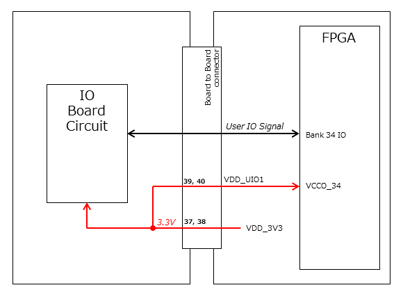
When using User IO at 3.3 V or when the IO Board consumes less than 0.3 A, VDD_3V3 can serve as the power supply.
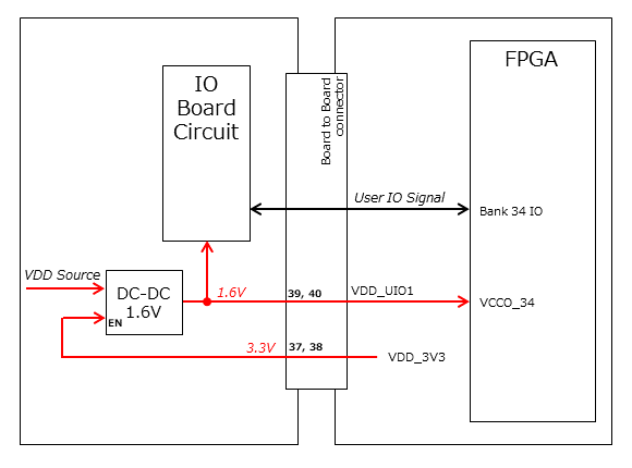
If User IO operates at 1.6 V or the IO Board’s current consumption is 0.3 A or more, use VDD_3V3 as the enable signal and provide power from the IO Board’s power supply.
4.1.3. Hardware Options and IO Connections
User IO Group 3 and WDOG_OUT signals can be routed to either TRCH or the FPGA, depending on hardware configuration. The connection configuration is fixed at shipment from Space Cubics and cannot be modified via software.
Please note that the signal power domain varies depending on whether it is connected to TRCH or the FPGA, so take care when designing the IO board.
| User IO | Endpoint when TRCH is selected | Endpoint when FPGA is selected |
|---|---|---|
UIO3_00 |
PIC16LF877 RD4/PSP4 |
FPGA IO_L23P_T3_12 (pin: Y15) |
UIO3_01 |
PIC16LF877 RD5/PSP5 |
FPGA IO_L23N_T3_12 (pin: AA15) |
UIO3_02 |
PIC16LF877 RD6/PSP6 |
FPGA IO_L24P_T3_12 (pin: W14) |
TRCH_UART_TX |
PIC16LF877 RC6/TX/CK |
FPGA IO_L24N_T3_12 (pin: W15) |
TRCH_UART_RX |
PIC16LF877 RC7/RX/DT |
FPGA IO_L1N_T0_12 (pin: AE26) |
WDOG_OUT |
PIC16LF877 RE0/AN5/RD |
FPGA IO_L16N_T2_12 (pin: AF18) |
-
Power domain
-
when TRCH is selected:
VDD_3V3_SYS -
when FPGA is selected:
VDD_3V3_IO
-
4.1.4. Debugger Connection
MPLAB PICkit4
TRCH software can be programmed using Microchip’s MPLAB and the PICKit4 debugger/programmer.
Connect MPLAB PICKit4 to the following pins on the OBC Module.
| MPLAB PICKit4 | OBC Module CON1 Pin No. |
|---|---|
1: MCLR |
51 |
2: VDD |
32 |
3: Ground |
6, 15, 24, 29, 33, 48, 52, 57, 66, 75 |
4: PGD |
49 |
5: PGC |
50 |
6: N.C. |
unconnected |
7: N.C. |
unconnected |
8: N.C. |
unconnected |
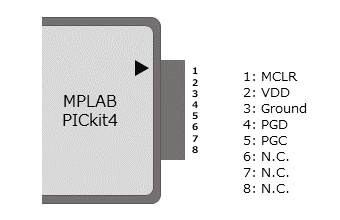
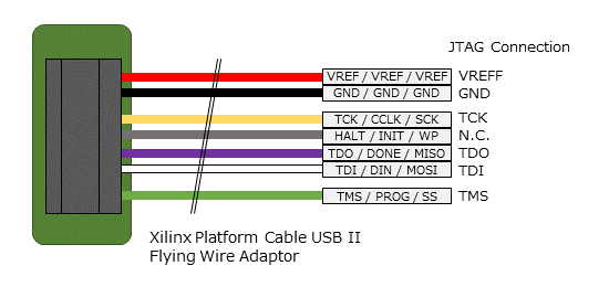
Platform Cable USB II
FPGA programming and in-circuit debugging can be performed using the Xilinx Platform Cable USB II.
Connect the USB II Platform Cable to the designated pins on the OBC module as shown below.
| Platform cable USB II | OBC Module CON1 Pin No. |
|---|---|
VREF |
OBC power signal (37, 38, etc.) |
GND |
6, 15, 24, 29, 33, 48, 52, 57, 66, 75 |
TCK |
53 |
HALT |
unconnected |
TDO |
54 |
TDI |
55 |
TMS |
56 |
5. OBC System Specifications
This section outlines the system specifications of the SC-OBC Module A1.
The SC-OBC Module A1 is composed of an FPGA, functioning as the main processor on the board, and a TRCH, which manages the system and operates in coordination with the FPGA. Users can customize the system freely by modifying both the FPGA logic and the TRCH program.
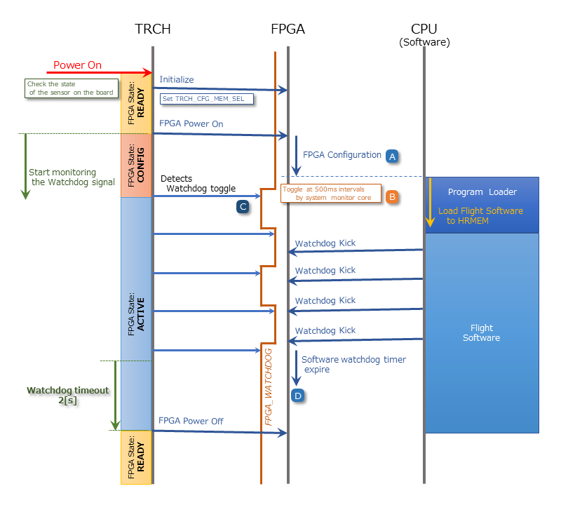
5.1. Power-on Operation
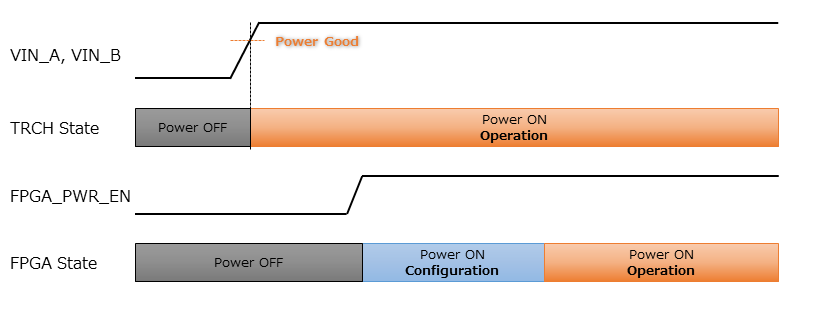
When power is applied to the OBC, the TRCH initializes first.
The TRCH monitors power status and temperature using sensors on the OBC board. If the conditions for FPGA operation are met, it sets FPGA_PWR_EN to HIGH to enable power to the FPGA.
When the FPGA is powered on, the TRCH uses the TRCH_CFG_MEM_SEL signal to select the memory for FPGA configuration. After power is applied, the FPGA reads data from the configuration memory selected by the TRCH and carries out its configuration.
5.2. FPGA Status Monitoring via TRCH
TRCH monitors the watchdog signal (FPGA_WATCHDOG) from the FPGA to detect issues with FPGA configuration or software operation.
When the TRCH powers up the FPGA, configuration begins immediately [A]. Once configuration is complete, the Watchdog circuit within the System Monitor implemented in the FPGA begins toggling the FPGA_WATCHDOG signal connected to the TRCH, independent of software operation [B]. The TRCH verifies that the OBC’s FPGA system is functioning correctly by checking that the FPGA_WATCHDOG signal toggles at regular intervals [C]. The System Monitor inside the FPGA detects that the Software Watchdog Timer has expired if the software fails to reset (kick) the timer within a set period (initially 128 seconds). When this happens, it stops toggling the FPGA_WATCHDOG signal [D].
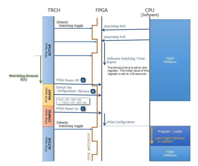
5.3. System Reboot
TRCH monitors the Watchdog and Power Cycle Request signals from the FPGA, then initiates the FPGA system power cycle when necessary.
If the FPGA software fails to trigger the Software Watchdog Timer within a specified time due to a problem in the FPGA system, the FPGA_WATCHDOG signal stops toggling after a set period. When TRCH detects that the FPGA_WATCHDOG signal has stopped, it switches off the FPGA power [A].
Before turning the FPGA power back on, the TRCH changes the configuration memory used by the FPGA [B]. This feature enables the FPGA to boot using data from a different configuration memory upon restart. After the configuration memory is switched, the FPGA is powered on again to complete the power cycle [C].
Changes to configuration memory occur both when a fault is detected by the watchdog and when the system is restarted in response to a power cycle request signal from the FPGA. When performing On the Fly rewriting of the configuration memory, if the new data causes a startup failure, the system will automatically restore the original configuration memory by rewriting it for the next startup and issuing a Power Cycle Request.
6. Board Status Circuit
The OBC Module has a function to monitor the OBC board status (power and temperature).
6.1. Power Status Monitoring
A Current and Voltage Monitor is integrated into the power supply nodes provided by the OBC Module. The Current and Voltage Monitor IC uses a TEXAS INSTRUMENTS INA3221-Q1 to communicate with both the TRCH and FPGA through an I2C interface, providing power data readings.
The monitoring nodes for the Current and Voltage Monitor are specified as follows.
| Current/Voltage Monitor No. | Slave Address | Channel | Node |
|---|---|---|---|
1 |
0x40 |
1 |
VDD_1V0 |
2 |
VDD_1V8 |
||
3 |
VDD_3V3 |
||
2 |
0x41 |
1 |
VDD_3V3_SYS_A |
2 |
VDD_3V3_SYS_B |
||
3 |
VDD_3V3_IO |
For details on accessing the Current and Voltage Monitor, please consult the INA3221-Q1 datasheet.
6.2. Temperature Monitoring
The OBC Module includes three temperature sensors to monitor temperature. The temperature sensor IC uses a TEXAS INSTRUMENTS TMQ175-Q1, which communicates with both the TRCH and FPGA via an I2C interface.
The mounting position and slave address for the temperature sensors are as follows.
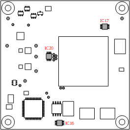
| IC No. | Slave Address |
|---|---|
IC16 |
0x4C |
IC17 |
0x4D |
IC20 |
0x4E |
